Search Your Query

Custom Search
Showing posts with label Microcontroller Based Project. Show all posts

Saturday, 17 September 2011

IR transmitter using AT89C2051

Hello dear friends
If you are trying to design an IR transmitter very similar to your TV remote control. I can help you in achieving this task. Here is program and circuit diagram. it use pin 3.3 (pin 7) of micro controller. Use the given simple program and check it from oscilloscope that it will transmit modulated 38KHz signal.
Circuit diagram is given below

Here is program you can run it using software for assembly language and then create file. After that burn hex file in your microcontroller.


;IR Transmitter using 89c2051

Program

ORG 0000H


Start:
IR EQU P3.3          ;IR trx CONNECTED TO THIS PIN

 
MOV TMOD,#00010001B ; TIMER-0, MODE 1 TIMER-1, MODE 1

sjmp MAIN


;--------------------------;-------------------------------------
;--------------------------;-------------------------------------


ONE:
MOV    TL1,#0CAH ;LOWER BYTE 1.728 MSEC
MOV    TH1,#0F9H ;UPPER BYTE
SETB  TR1
HERE:
MOV    TL0,#0F4H ;LOWER BYTE 38 KHZ
MOV    TH0,#0FFH ;UPPER BYTE
SETB  TR0
CPL   IR
JNB  TF0,$
CLR   TF0
JNB   TF1,HERE
CLR   TF1
Clr IR
RET
;--------------------------;-------------------------------------
;--------------------------;-------------------------------------


;--------------------------;-------------------------------------
;--------------------------;-------------------------------------
ZERO:
MOV    TL1,#0CAH ;LOWER BYTE 1.7728 MSEC
MOV    TH1,#0F9H ;UPPER BYTE
SETB  TR1
SetB  IR
JNB   TF1,$
CLR   TF1
Clr IR
RET
;--------------------------;-------------------------------------
;--------------------------;-------------------------------------


;--------------------------;-------------------------------------
;--------------------------;-------------------------------------
MAIN:
Acall ONE
Acall ZERO
Sjmp MAIN


;--------------------------;-------------------------------------
;--------------------------;-------------------------------------

END


Friday, 16 September 2011

Servo Motor Tester Circuit and Programming using AT89C2051

Here is the program to control simple servo motor in both direction. I test it today and think that i should also share it with you people so that you can also enjoy and can take benefit. This program will rotate servo motor in both clock wise and anti clock wise direction you can modify it according to your requirement and according to your wish as suite to you.
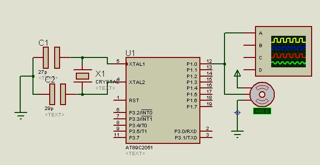
 Here is Proteus schematic layout.

Simple you need in this circuit one AT89C2051.
One 11.0592MHz crystal connect it to pin 4 and pin 5
29pF capacitors
One servo motor
connect all as shown in figure above.
After that use Keil software or any other software which you know how to use it for assembly language  run this program and create hex file
and make changes as you wish then burn it into your controller and enjoy......

Program for Servo motor


;***SERVO MOTOR FREE CLK & ANTI CLKWISE ***
;OUTPUT=P1.0
;CRYSTAL=11.0592MHz

ORG 00H
MAIN:
MOV R2,#0FAH
MOV R3,#03H
RUNN:
ACALL START
DJNZ R3,RUNN
MOV R3,#0FFH
DEC R2
MOV A,R2
CJNE A,#0F6H,RUNN
RUNN1:
ACALL START
INC R3
MOV A,R3
CJNE A,#0FFH,RUNN1
MOV R3,#0H
INC R2
MOV A,R2
CJNE A,#0FEH,RUNN1
MOV R3,#05H
SJMP RUNN


START:
MOV TMOD,#11H
MOV TH0,#0FBH
MOV TL0,#0FBH
SETB TR0
CLR P1.0
AGAIN:
JNB TF0,$
CLR TF0
CLR TR0
HIGH1:
MOV TH1,R2
MOV TL1,R3
SETB P1.0
SETB TR1
AGAIN1:
JNB TF1,$
CLR TF1
CLR TR1
RET
END

Monday, 30 May 2011

Digital Code lock using AT89C2051


Here is a project called ‘Digital Code Lock using AT89C2051′. LCD is used for display and a keyboard is used to input  the keys. This project source code is written in C. Both the C files and hex files are given for download.
A Brief Description:
This a simple project with efficient hacking prevention from Brute Force etc. The basic user lock is of 5 Digits and Master Lock is of 10 digits so its not easy for an intruder to break the lock unless you keep the code simple.
The input is taken from a 4×3 Keypad (please see the schematic for more information) and Display the user input on a 2×16 LCD. A pin is assigned as output for activating and deactivating the lock. For demonstration i have connected an LED to that pin.
From user side:
The user has two options either he/she can use its own 5 digit code or use the default 5 digit code. If user has to do setup his own code, then he has to enter “12345″ and press ‘#’. After this.. controller will ask for 10 Digit master password which is preprogrammed in the controller. Entering master lock, user can enter the new 5 digit code for the lock and press ‘#’ to save it.
Using the Keypad:
Keypad has 12 keys (4×3) starting from 1,2,3,4,5,6,7,8,9,*,0,# (please see the schematic for layout). Numeric keys are used for entering numbers. ‘*’ is used as the Cancel key and ‘#’ is used as the Enter key.
Circuit Diagram:
Circuit diagram of Digital Code lock using AT89C2051
Download File Information:
  1. LCD.C – 4-Bit LCD Drivers
  2. LCD.H – LCD function prototypes and other declerations
  3. Lock.C – code for lock functioning
  4. LOCK.H – lock function declarations
  5. KEYPAD.C – Keypad drivers
  6. KEYPAD.H – Function declarations
  7. DELAY.C – Delay Functions
  8. DELAY.H – Function Prototypes only
  9. MAIN.C – Main function!
  10. Digital Code Lock Schematic – PDF file of orcad schematic
Download the source codes by clicking here

Programmable number lock system


Programmable number lock system is a high security number lock system that can be used to lock electronic devices. The present system is very user friendly. This system is a combination of software and hardware at its best. We have used a 8051 microcontroller kit for interfacing our system.
In the present design we can activate or deactivate 9 devices. Each device is locked using a 4 digit code (password). The code can be set as per the user’s desire, hence the name ‘ PROGRAMMABLE ‘. For the device to be activated (unlocked), the user should enter the code that had been entered when the device was locked. In case the user enters the wrong code a silent alarm will be activated.
Introduction to Programmable number lock system:
The system has three units, namely:
  1. Keyboard unit.
  2. Display unit.
  3. Control unit.
The keyboard unit consists of 9 number keys, 1 unlock key and 1 lock key. These are all push button switches. This unit is used to select the desired device and to enter the codes into the system. It is also used to request the system to lock/unlock the selected device.
The display section contains 5 seven segment display. This unit displays the device number and the code entered. This section is detachable. If detached it does not affect the working of the whole system. This unit also contains password reset button and an LED to indicate the error when the device is   already locked and user wants to lock the device again. The error indicator also indicates an error when the system is already unlocked and the user tries to unlock the same.
The control unit  is the heart of our system. It contains the necessary circuitry for the control of the device .This unit controls 9 devices, which is lock/unlock  by selecting it using the keyboard and entering the password. If the code entered to unlock the device is wrong, then a silent alarm is triggered .The keyboard unit and the display unit are connected to this unit.
All these three units are merged together to form the whole system.
Model of Programmable number lock system
Block diagram of Programmable number lock system:
 Block diagram of Programmable number lock system:
Block diagram of Programmable number lock system:
Working of the system:
When the system  is initially installed the reset button is pressed. This key is present in the control unit. This unlocks all the devices. This is to avoid undesired functioning of the system.
To lock a particular device the device number is selected using the keyboard. Once the device is selected the user has to press the lock key present in the keyboard. Now the device waits for the user to enter the the code. The user can enter a 4 digit number using the keyboard as per his desire. Once all the 4 digits are entered the system electronically locks the selected device.
In the same manner to unlock a particular device, the device number is entered using the keyboard. Once the device number is selected the code for the selected device is entered. If the entered code matches the code that had been entered while that particular device was locked then the selected device will be activated (unlocked). If the codes do not match each other a silent alarm will be triggered (a LED placed in the control section. Shown in figure 3).An error indicator (placed in the display section) is provided if any user tries to lock a device which has already been locked or vice versa.
If the user is half way entering the code or has done an error while entering the code and wants to start over all again then a reset button is provided in the display section. By pressing this button the user can start from entering the device number and so on.
The number of devices which the system can control can be increased by addition of a few components in the control unit. More security can be achieved by increasing the number of digits in the code. This can be done by minor changes in the program. The system uses the internal RAM of the 8051 to store the code and hence puts a lower limit to the number of digits in the code and also the number of devices the system can control. Once the system is installed only the display unit and keyboard unit will be accessible to the user. Access to the control unit should be provided only to an official personal since it contains the system  reset button.
System:
In this section we will be explaining the hardware design these units individually. Each unit description is accompanied by its circuit diagram.
KEYBOARD UNIT :
The keyboard used in this system is an encoder type. It uses IC 74147 priority encoder to convert the entered the digits to its corresponding binary codes. IC 74147 has a active low inputs as well as active low outputs (for more details please refer the corresponding data sheets). Each of the pins are activated using push to on switches. These switches ground the encoder inputs to activate that particular number giving the equivalent BCD code. This is then given as input to IC 7404 which is an inverter. To avoid loading of 7404 by the later stages transistor switches are provided to each of its outputs. The circuit diagram of the keyboard is as given in the next section.
Circuit diagram of Keyboard section
DISPLAY UNIT :
The logic used here is shift and display i.e. when the next number is entered the previous number is shifted to the left by one unit and then the next number is displayed. To achieve this we have used IC 7496 which is a 5–bit shift register (for more details please refer the corresponding data sheets). The data lines from control section are given serially to the registers as shown in the circuit. The clock to these registers is given by the program every time a button on the keyboard is pressed. The shifting used here is parallel shifting. The outputs of the registers are given to CD4511 BCD to seven segment decoder. The seven segment display used are common cathode type since the output of the decoder is high when activated. This section consists of a reset switch which is used to reset the display.
Circuit diagram of Keyboard section
Control unit:
Circuit diagram of Control Unit
The program codes for this project is given in the next page
APPLICATION:
The ‘Electronic device number lock’ system is a high security system.The main application kept in mind during the design of this system is to secure expensive electronic devices and machinery. The access to such devices can be restricted to particular users only. The system is highly secured since the code can be changed every time the user locks it.
This can also be used an physical lock by using solenoid and thus can be used to lock safes in banks or other institutions.
Regular electronic number lock available in the market can lock/unlock just one device, but this design can lock/unlock up to nine devices.
The program used for the operation of this system is as follows :
;***************************************************************;
PROCEDURE OF WAIT
;***************************************************************
org 8500h
wait:  push dph
push dpl
push r0
push r1
mov dptr,#2042h     ;input data from PORT C
wi:     movx a,@dptr
mov r2,a
anl a,#20h
jz cont                      ;check for interrupt from display unit
jmp start
cont:  mov a,r2
anl a,#0fh                ;to check whether any key is pressed
jz wi
mov r0,#75
lcall 6798h
mov dptr,#2042h
here:  movx a,@dptr          ;wait for the key to be realesed
jnz here
mov dptr,#2040h     ;sending a pulse to the display section
mov a,r2
movx @dptr,a
mov a,#00h
mov dptr,#2041h
movx @dptr,a
mov a,#40h
movx @dptr,a
mov a,r2
mov r0,#75
lcall 6798h
pop r1
pop r0
pop dpl
pop dph
ret
;***************************************************************;
STORING  AND RETRIVING OF PASS WORD
;***************************************************************
org 8550h
scan:  mov r0,#04h
mov dptr,#2042h
one:  movx a,@dptr      ;check for lock or unlock buttons
anl a,#0c0h
jz one
ret
lock:  lcall  wait             ;storing of pass word in given location
mov @r1,a
inc r1
djnz r0,lock
lcall out
ret
unlock: clr 0ah
call wait
mov a,@r1
xrl a,r2                 ;comparing the entered and the stored code
jz match
setb 0ah              ;in case of mismatch set error bit
match: inc r1
djnz r0,unlock
jnb 0ah,go
mov a,#20h
push dptr
mov dptr,#2040h
movx @dptr,a
push r0
push r1
mov r0,#ffh
lcall 6798h
pop r1
pop r0
mov a,#00h
movx @dptr,a
pop dptr
jmp not
go:    lcall out
not:   ret
;***************************************************************;
TO ACCEPT THE DEVICE NUMBER
;***************************************************************
org 9000h
mov sp,#05fh
main:  clr 01h                        ;clearing all the device flags
clr 02h
clr 03h
clr 04h
clr 05h
clr 06h
clr 07h
clr 08h
clr 09h
setb ie.7
setb ie.2
start: mov a,#89h                ;C as ip,A and B as op
mov dptr,#2043h
movx @dptr,a
mov r7,#05h               ;clearing the display section
rss:   mov dptr,#2040h
mov a,#00h
movx @dptr,a
mov a,#00h
mov dptr,#2041h
movx @dptr,a
mov a,#40h
movx @dptr,a
djnz r7,rss
lcall wait
cjne a,#01h,nxt2
jmp dev1
nxt2: cjne a,#02h,nxt3
jmp dev2
nxt3: cjne a,#03h,nxt4
jmp dev3
nxt4: cjne a,#04h,nxt5
jmp dev4
nxt5: cjne a,#05h,nxt6
jmp dev5
nxt6: cjne a,#06h,nxt7
jmp dev6
nxt7: cjne a,#07h,nxt8
jmp dev7
nxt8: cjne a,#08h,nxt9
jmp dev8
nxt9: cjne a,#09h,start
jmp dev9
;***************************************************************;
SELECTED DEVICE ACTIVATION
;***************************************************************
org 9200h
dev1: mov r1,#30h               ;Loading the address of the password
mov r3,#01h                ;device no. used to give to the decoder
lcall scan
cjne a,#80h,unlock1    ;check for the lockunlock pressed
jmp lock1
unlock1: jnb 01h,error1         ;generating error if the selected device is already
;activated
lcall unlock
jb 0ah,hr1
clr 01h                          ;clear lockunlock flag
hr1:   jmp start
lock1: jb 01h,error1
lcall lock
setb 01h                       ;set lockunlock flag
jmp start
error1: mov a,#40h              ;activating the error LED
mov dptr,#2040h
movx @dptr,a
push dptr
push r0
push r1
mov r0,#ffh
lcall 6798h
pop r1
pop r0
pop dptr
jmp start
;***************************************************************
dev2: mov r1,#035h
mov r3,#02h
lcall scan
cjne a,#80h,unlock2
jmp lock2
unlock2: jnb 02h,error2
lcall unlock
jb 0ah,hr2
clr 02h
hr2:   jmp start
lock2: jb 02h,error2
lcall lock
setb 02h
jmp start
error2: mov a,#40h
mov dptr,#2040h
movx @dptr,a
push dptr
push r0
push r1
mov r0,#ffh
lcall 6798h
pop r1
pop r0
pop dptr
jmp start
;***************************************************************
dev3: mov r1,#03ah
mov r3,#03h
lcall scan
cjne a,#80h,unlock3
jmp lock3
unlock3:jnb 03h,error3
lcall unlock
jb 0ah,hr3
clr 03h
hr3: jmp start
lock3:jb 03h,error3
lcall lock
setb 03h
jmp start
error3: mov a,#40h
mov dptr,#2040h
movx @dptr,a
push dptr
push r0
push r1
mov r0,#ffh
lcall 6798h
pop r1
pop r0
pop dptr
jmp start
;***************************************************************
dev4: mov r1,#040h
mov r3,#04
lcall scan
cjne a,#80h,unlock4
jmp lock4
unlock4:jnb 04h,error4
lcall unlock
jb 0ah,hr4
clr 04h
hr4:   jmp start
lock4:jb 04h,error4
lcall lock
setb 04h
jmp start
error4: mov a,#40h
mov dptr,#2040h
movx @dptr,a
push dptr
push r0
push r1
mov r0,#ffh
lcall 6798h
pop r1
pop r0
pop dptr
jmp start
;***************************************************************
dev5: mov r1,#045h
mov r3,#05h
lcall scan
cjne a,#80h,unlock5
jmp lock5
unlock5:jnb 05h,error5
lcall unlock
jb 0ah,hr5
clr 05h
hr5:   jmp start
lock5:jb 05h,error5
lcall lock
setb 05h
jmp start
error5: mov a,#40h
mov dptr,#2040h
movx @dptr,a
push dptr
push r0
push r1
mov r0,#ffh
lcall 6798h
pop r1
pop r0
pop dptr
jmp start
;***************************************************************
dev6: mov r1,#04ah
mov r3,#06h
lcall scan
cjne a,#80h,unlock6
jmp lock6
unlock6:jnb 06h,error6
lcall unlock
jb 0ah,hr6
clr 06h
hr6:   jmp start
lock6:jb 06h,error6
lcall lock
setb 06h
jmp start
error6: mov a,#40h
mov dptr,#2040h
movx @dptr,a
push dptr
push r0
push r1
mov r0,#ffh
lcall 6798h
pop r1
pop r0
pop dptr
jmp start
;**************************************************************
dev7: mov r1,#050h
mov r3,#07h
lcall scan
cjne a,#80h,unlock7
jmp lock7
unlock7:jnb 07h,error7
lcall unlock
jb 0ah,hr7
clr 07h
hr7:jmp start
lock7:jb 07h,error7
lcall lock
setb 07h
jmp start
error7: mov a,#40h
mov dptr,#2040h
movx @dptr,a
push dptr
push r0
push r1
mov r0,#ffh
lcall 6798h
pop r1
pop r0
pop dptr
jmp start
;***********************************************************
dev8: mov r1,#055h
mov r3,#08h
lcall scan
cjne a,#80h,unlock8
jmp lock8
unlock8:jnb 08h,error8
lcall unlock
jb 0ah,hr8
clr 08h
hr8:   jmp start
lock8:jb 08h,error8
lcall lock
setb 08h
jmp start
error8: mov a,#40h
mov dptr,#2040h
movx @dptr,a
push dptr
push r0
push r1
mov r0,#ffh
lcall 6798h
pop r1
pop r0
pop dptr
jmp start
;***********************************************************
dev9: mov r1,#05ah
mov r3,#09h
lcall scan
cjne a,#80h,unlock9
jmp lock9
unlock9:jnb 09h,error9
lcall unlock
jb 0ah,hr9
clr 09h
hr9: jmp start
lock9:jb 09h,error9
lcall lock
setb 09h
jmp start
error9: mov a,#40h
mov dptr,#2040h
movx @dptr,a
push dptr
push r0
push r1
mov r0,#ffh
lcall 6798h
pop r1
pop r0
pop dptr
jmp start
;***********************************************************
;                    OUTPUT SECTION
;***********************************************************
org 0a000h
out:   mov a,r3         ;loading the device number
mov dptr,#2041h
movx @dptr,a
ret
;***********************************************************
This program is assembled using DASM assembler and the hex file is downloaded to the 8051 microcontroller kit.

Related Posts Plugin for WordPress, Blogger...